Case study: Building a MIDI controller (part 1)
Why I did this
I did this whole thing for three reasons:
- I want to learn more about electrical engineering and designing PCBs
- I wanted to test our platform and its features
- I want to know if current AI is helpful in this area, or if it mostly just messes things up
I’m not an electrical engineer. I’m a programmer. BUT I learned basic electronics at uni, and I have a basic understanding of the area, so this post will not be a “Create a PCB! Make no mistakes!” prompt where we watch it burn together.
I used Claude (Opus 5.5 and Fable 5.1).
I’m still in the “doing” phase, so some of what follows may be overridden in the next parts.
The project idea
I’m interested in MIDI controllers. I have an Akai MPK mini MK3 and I like it, but before that I almost bought an LPD8, and if I had money that I wanted to “waste”, I would probably buy a bunch of Intech devices, because they look really nice tech-wise. So, why not build one for myself? Also, current mechanical keyboard tech with hall sensors, where you can measure velocity and tell the press depth, opens up a lot of options (or I hope so, we will see).
So the idea started as:
- 8 hall sensor mechanical switches (Gateron KS-20)
- 8 encoders (copying the LPD8, they are smart, don’t reinvent the wheel)
- one screen (for settings and stuff)
- LEDs under every key, and maybe next to every encoder
- USB-C, it should show up as a MIDI device when I plug it in
- I’m not really good at soldering, so use as many LCSC components as possible, so JLCPCB can assemble at least the SMD parts for me
As I started to browse, I added two more encoders, and I chose an ESP32-S3, so I have the option to use Bluetooth and to configure/monitor it over Wi-Fi if I ever want to.
The final idea is that if we rotate the thing 90 degrees, we can map the 8 keys to effects and use the 10 encoders for DJing too, while in the standard orientation it’s a simple MIDI controller for DAWs.
The name of the project is Hale H8E10: H8E10 as in 8 (hall) keys and 10 encoders. Keep the naming scheme in mind, it comes back at the end. The project is public on pcbjam, so you can open it and follow along.
The ideation phase
I used the chat mode on mobile, not Claude Code. It was kinda ok. The very first idea used Behringer X32 replacement faders because they seemed super cool, but we agreed that for a first project, and to fit comfortably into the USB power budget, we should make something simpler. (A motorized fader could eat 8W at peak, which is a LOT.)
I described the idea, asked about symbol/footprint/3D model availability, part lookups, pin numbers, etc. I asked “how would you do it” and “why” questions a lot. We agreed on the hall sensors, switches, ADCs, GPIO expanders and LEDs, we tried to find a suitable screen, and we checked some better quality encoders too. We also talked about usability: what settings we should have, and what can be achieved in software.
When everything felt ok, I asked it to wrap everything into a “project”, we argued about what a good name for a project like this looks like, then I made my first commit, and we moved to Claude Code.
In general Claude is good for ideas. If you ask the right questions, it will support your decisions. BUT ideas are cheap, as the next section shows.
Data gathering and planning phase
I’m a noob. So I started by gathering datasheets, and as we progressed, we found out that some of our initial “ideas” didn’t really meet reality.
KS-20
Let’s start with the hall sensors and the PCB thickness. We initially assumed that we would have problems detecting the KS-20 magnets. We agreed on the SS39ET as the hall sensor, and a 1.2mm PCB. Then we read the datasheets, I asked Claude the right question “by chance”, and we found the following:
- KS-20 has 102 ± 15 G at rest and 905 ± 80 G at full press
- Gateron probably measured these numbers through a “standard” 1.6mm board
- the SS39ET clips at about 520-780 G on 3.3V
- the magnetic field drops off steeply with distance, so because of the clipping we would lose about 0.2-1.2mm of the 4mm travel
- running the SS39ET from 5V could help a bit, but then 5V rail noise would become a whole new problem space
Claude made multiple small mistakes here. For example, it didn’t read the BOM.md, so it “forgot” that we wanted to use an ADC (I made it write this into the CLAUDE.md so the next session won’t make the same mistake). It also found that some of the LCSC part numbers from before were totally off, and tried to fix them (I didn’t check these, we are not yet at the point where it matters).
We did a quick search and found out that Gateron doesn’t have a recommended sensor. Claude checked some OSS projects and found that some of them still use the sensor we chose, and all of them use 1.6mm boards. We chose a secondary sensor option, the DRV5055A3QDBZR, and noted that we should check the footprints and make them interchangeable. (In theory they are interchangeable, but we will come back to this later…)
Screens, case, 3D modeling
I’m a programmer, so I like everything that is code-driven. I made a lot of models in OpenSCAD, but lately I started to use FluidCAD. AI can drive it, a human can check it, and I can change it in code, refactor it or parametrize it if needed. So I downloaded the drawings of the chosen screen, gave them to Claude, and it made a 3D model. And here are my two cents. It looked ok. It looked like it matched the drawings. But it did NOT! After I checked EVERY distance, I found two bugs. One was a drawing-reading problem: it misinterpreted some arrows, and when I pointed it out, it agreed with me. The second was the pin positions.
THE WORST thing that can happen is that your drills/cutouts don’t match the module you ordered, and that is exactly what happened here. It took two more iterations before we finally reached a mutual understanding. So my advice is to double-check EVERYTHING. (But when I asked if it could “skin” the screen, it did an excellent job, and added the texts and the pads too.)
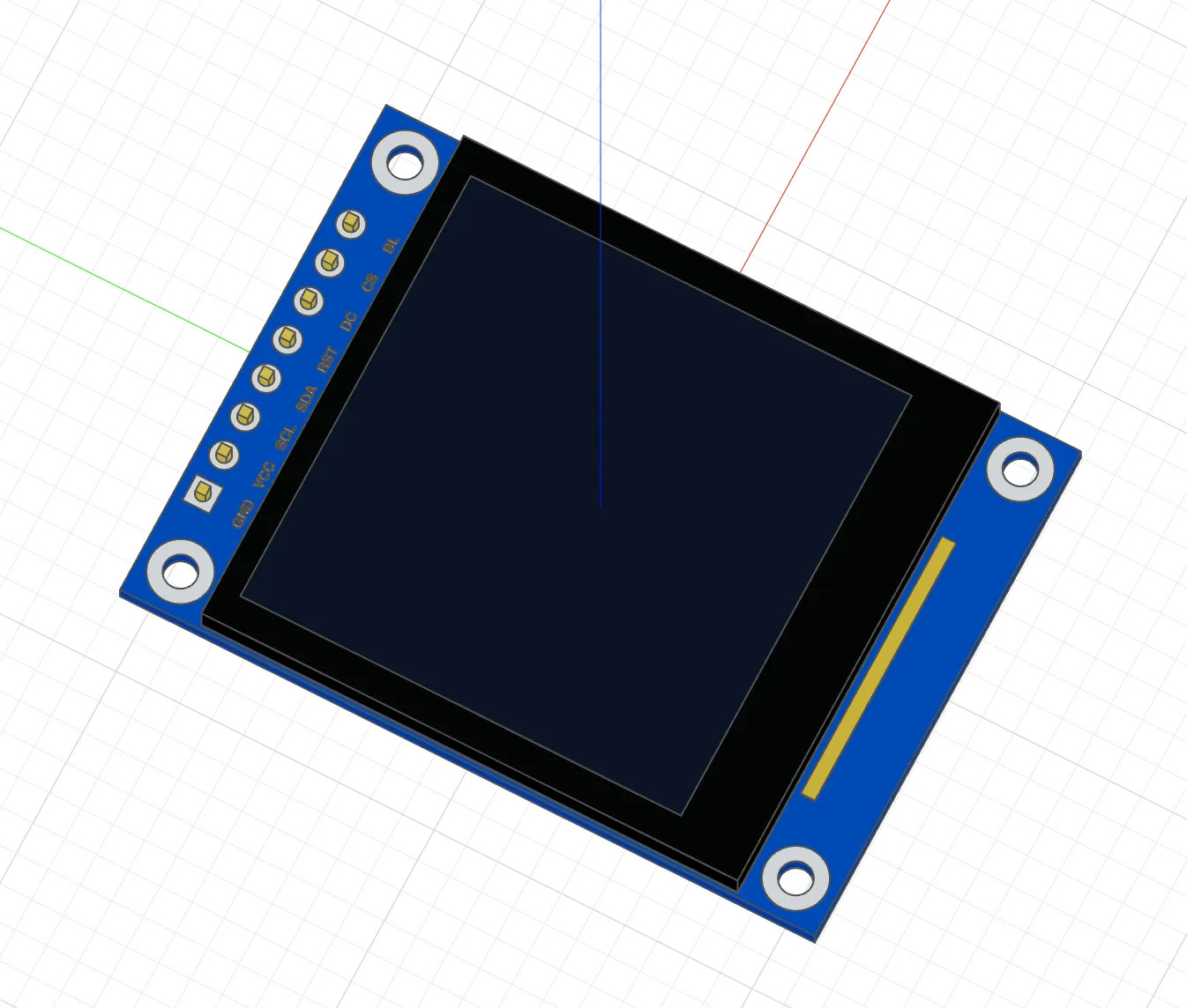
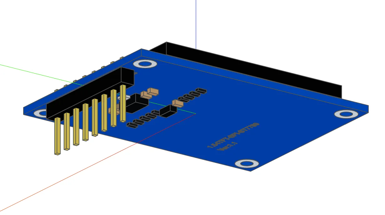
After we talked about the Alps and Bourns encoders, and decided that the threads and the 24 detents / 24 pulses favor Bourns, I asked it to model a full product. It was not bad (I don’t have screenshots), but then the second “reality” problem came in: the keys and the encoders take up totally different areas.
Encoders need somewhere between 20x20 and 30x30mm (Intech uses 26.75x26.75, we can learn from them), and keys need 19.05mm, so I can almost fit a 3rd row of keys. Or I can move the screen if I choose another one. So the first screen had to go. Back to AliExpress, searching for screens that fit in the “3rd key row”, have drawings and SPI, can work from 3.3V or 5V, and have a CS pin.
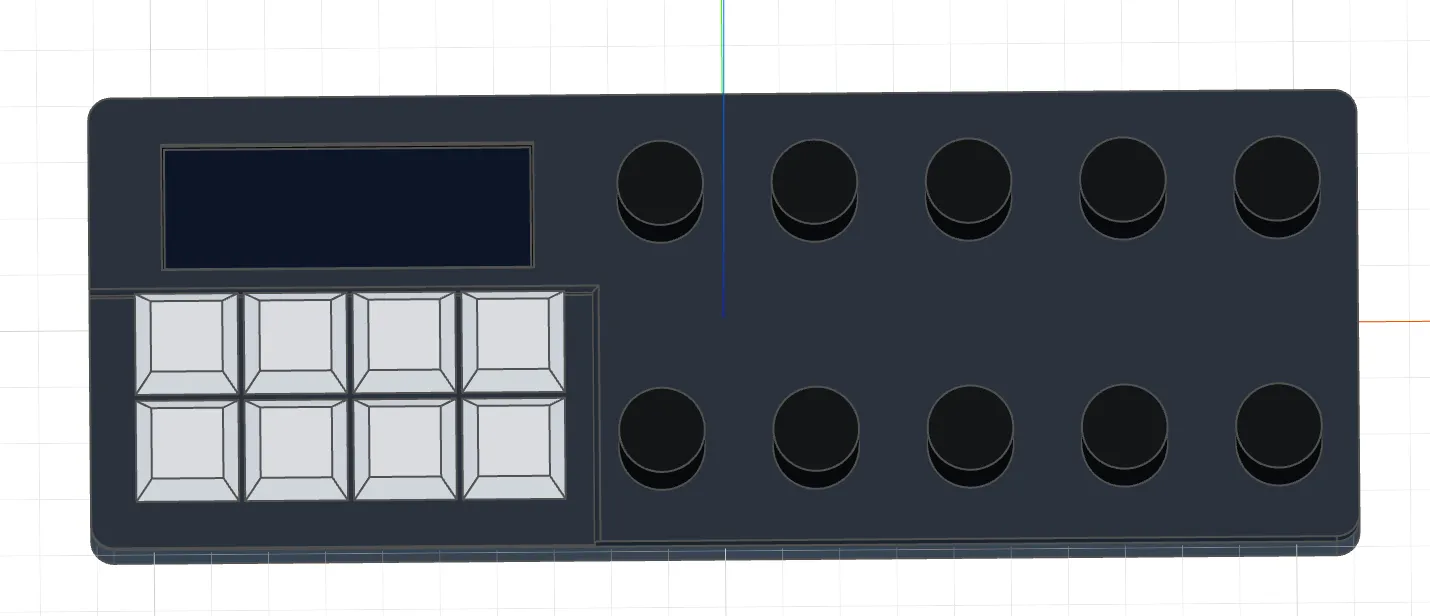
After some back and forth, this is the first render that I think looks okay. (I changed some placements since this screenshot was taken, but it’s a nice first try.)
Of course I needed to triple-check the new screen model against the screen drawings, but this time there was only a 0.01mm difference that neither I nor Claude could resolve from the drawings (1.66 vs 1.65). It will probably not matter, the pins move 0.01mm.
Symbols and schematic
For the schematic I needed to create two new symbols: the key (a simple rectangle, no pins) and the screen (8 pins). Both were really straightforward. I found some inconveniences in our platform while making the symbols and fixed them along the way (more on that at the end).
The schematic was less easy. We have 8 keys with LEDs, the LEDs need a capacitor, and each key needs a hall sensor. We have 10 encoders (with 2 capacitors each), and each needs an LED (with a capacitor). So I told Claude that I want a key cell and an encoder cell as sub-sheets, and I want to copy-paste those sheets. Then it came up with a LOT of sub-sheets, which I rationalized, and in the end we agreed on five:
- key cell (key, sensor, LED)
- encoder cell (encoder, LED)
- keys (8 keys, ADC, LDO)
- encoders (10 encoders, GPIO expanders)
- main (MCU, screen, keys, encoders, status LEDs)
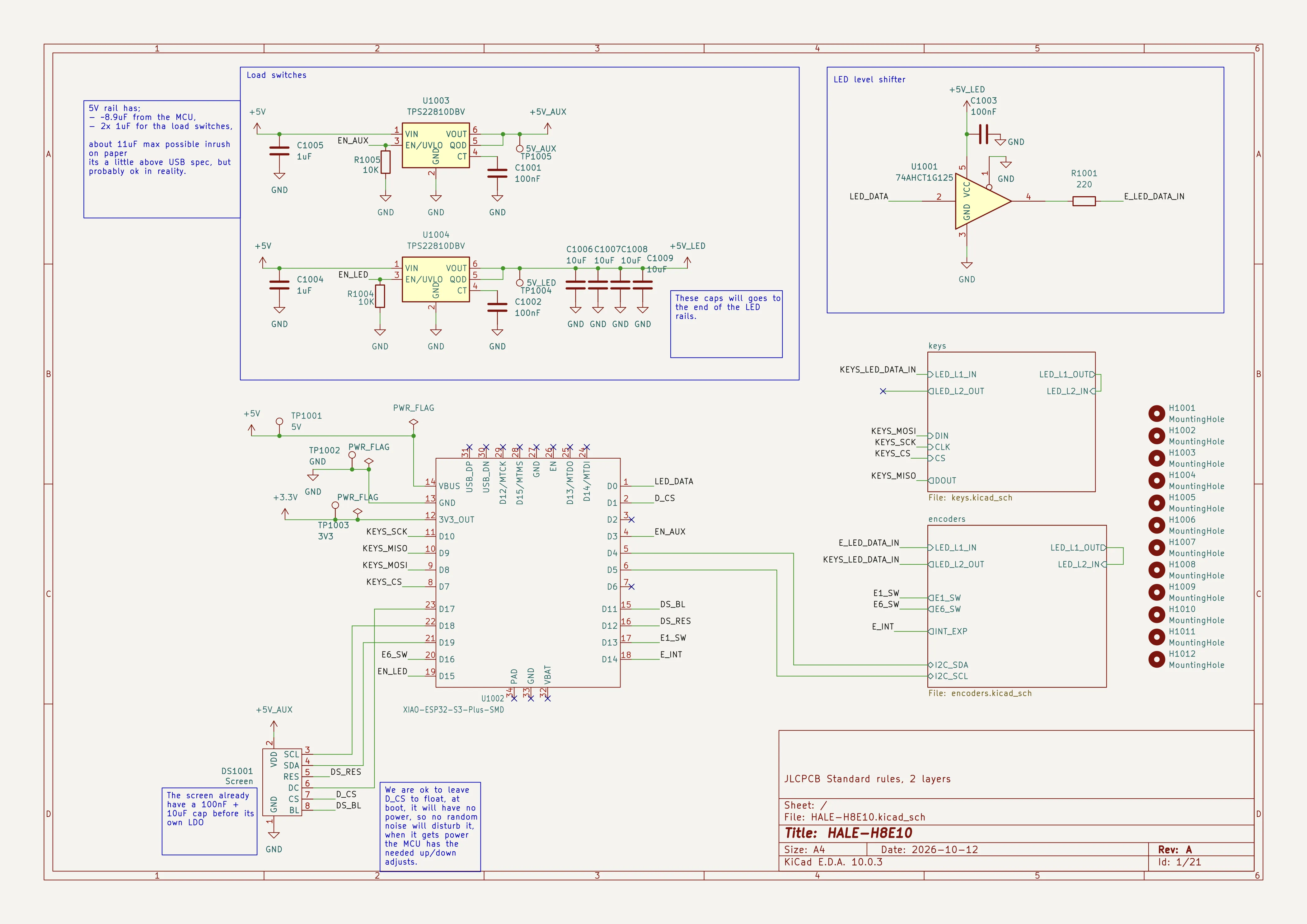
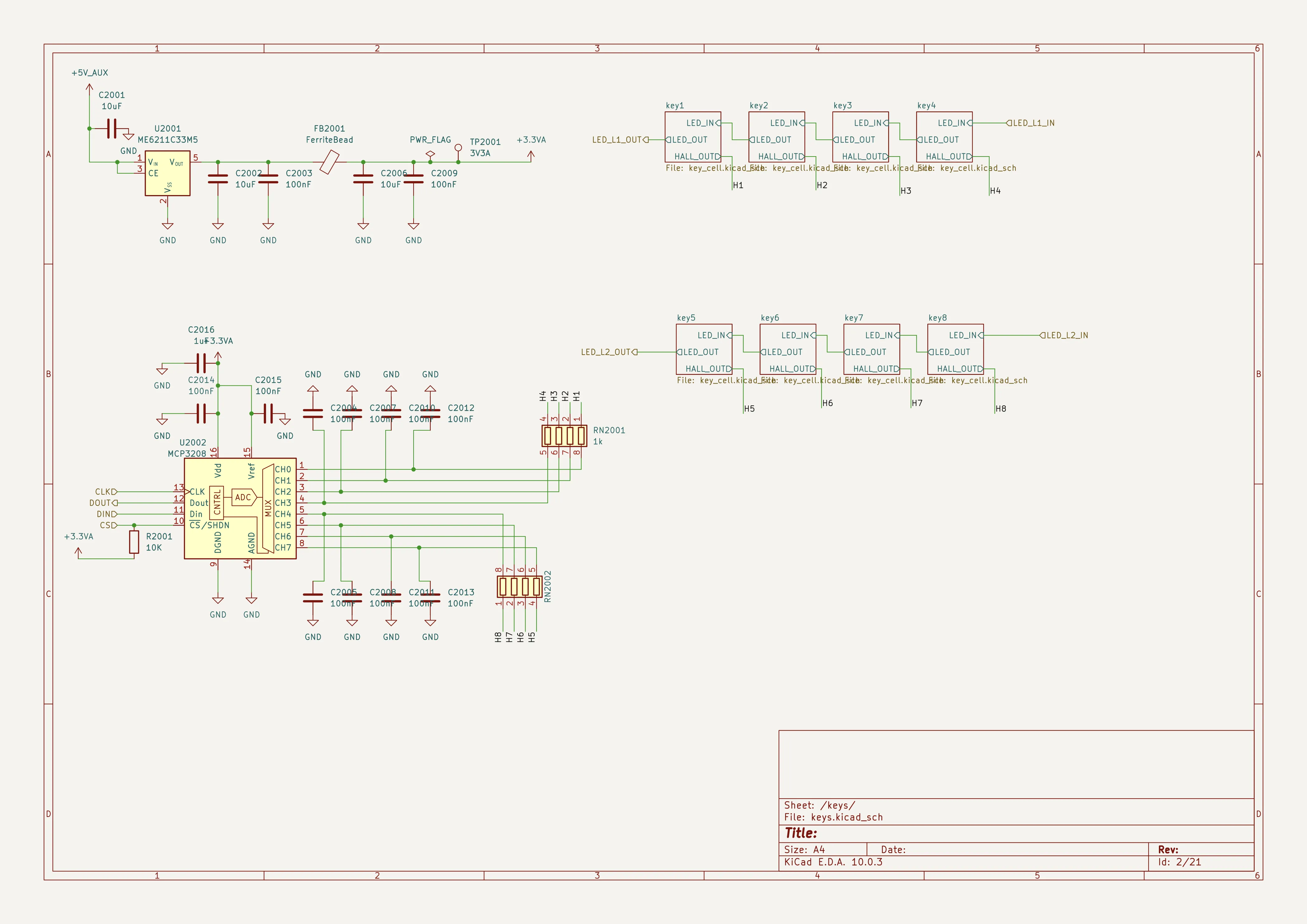
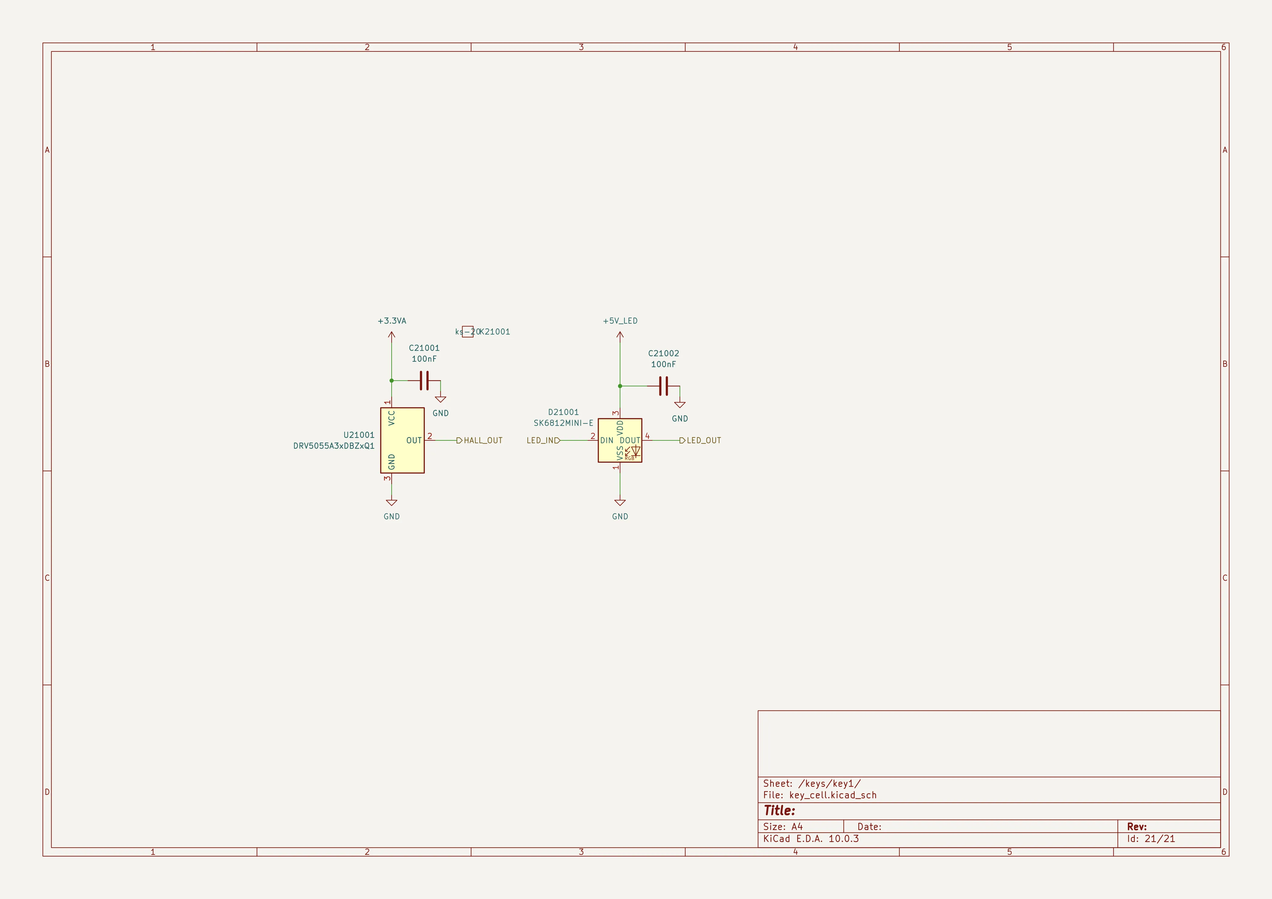
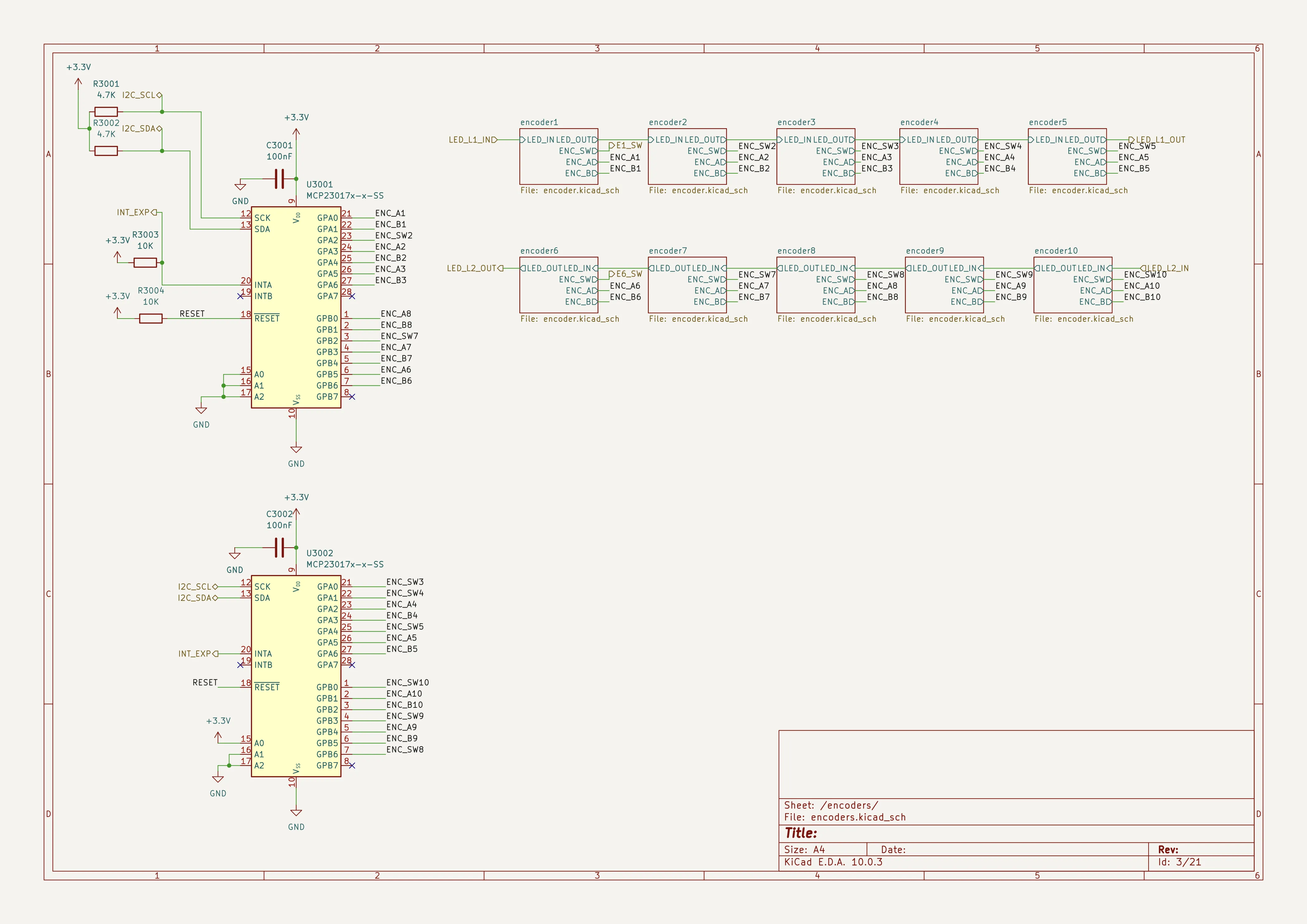
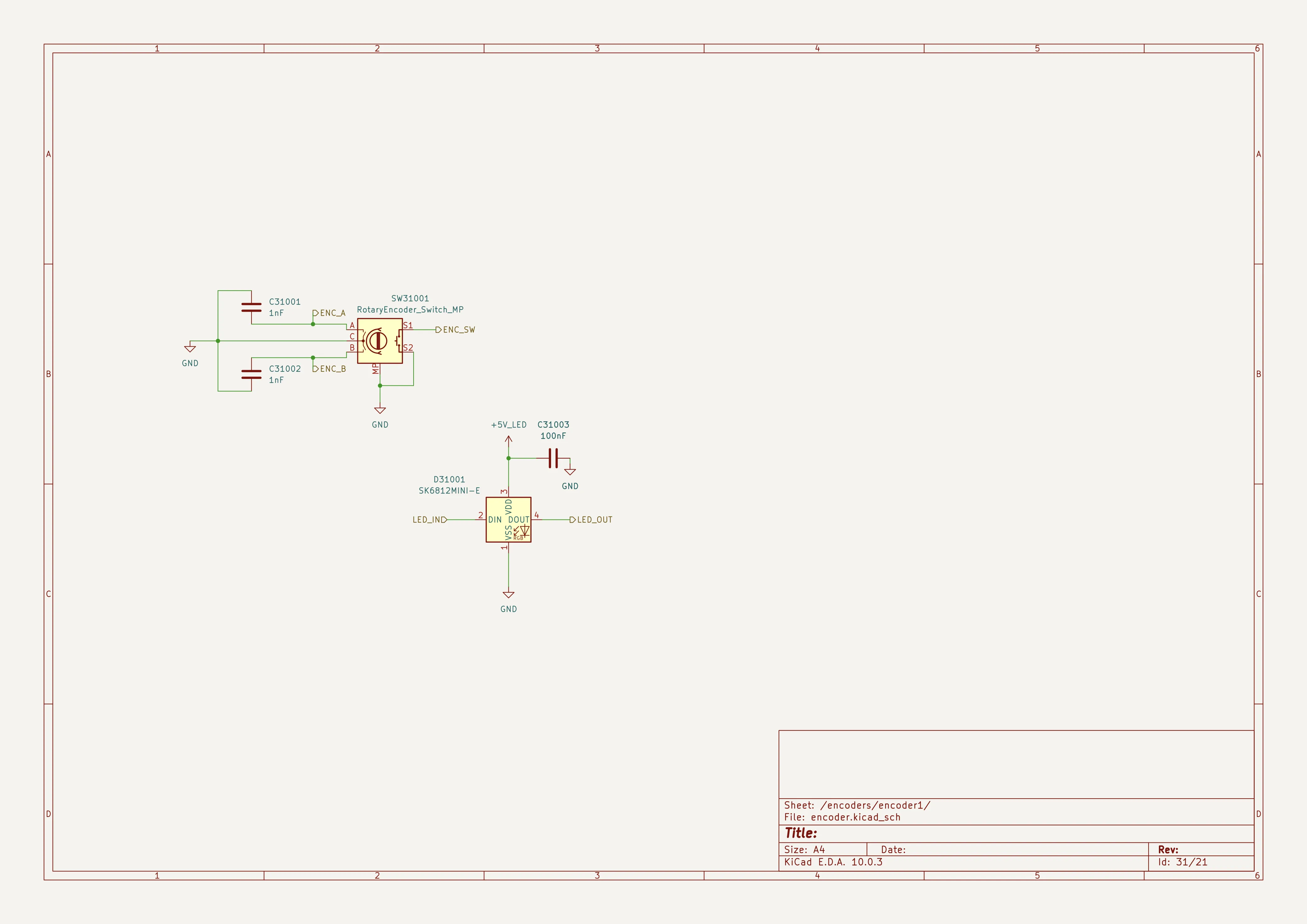
One thing I needed help with was sizing the capacitors and resistors. I still think we have too many, but I will check again when the whole thing comes together. I’m used to wiring things up on a breadboard, so it’s really strange to me that we need this many capacitors and pull-up/down resistors. But of course I would never call a breadboard a product, so I have to say that here the AI is stricter than I would have been by just reading Reddit/forum posts.
Footprints and PCB
Meanwhile, I started to draw footprints in parallel with the symbols, and it was a PAIN. First of all, even when I blindly followed Claude’s “draw a symmetric 35x24 rectangle on the courtyard”, it was really hard to do. It is probably a skill issue on my end, but moving things and placing them at exact positions in the footprint editor is really hard. According to the AI, I needed to draw three footprints: one for the KS-20 (the key), one for the display, and one for the hall sensors. The reasoning was that the two sensors differ a bit, and if we want to test both (DRV5055A3 and SS39ET), we should draw a “generic” footprint. And I was dumb enough to draw it…
Checking the datasheet drawings against the footprints was painful enough that I built and deployed a checking tool for it (see the end).
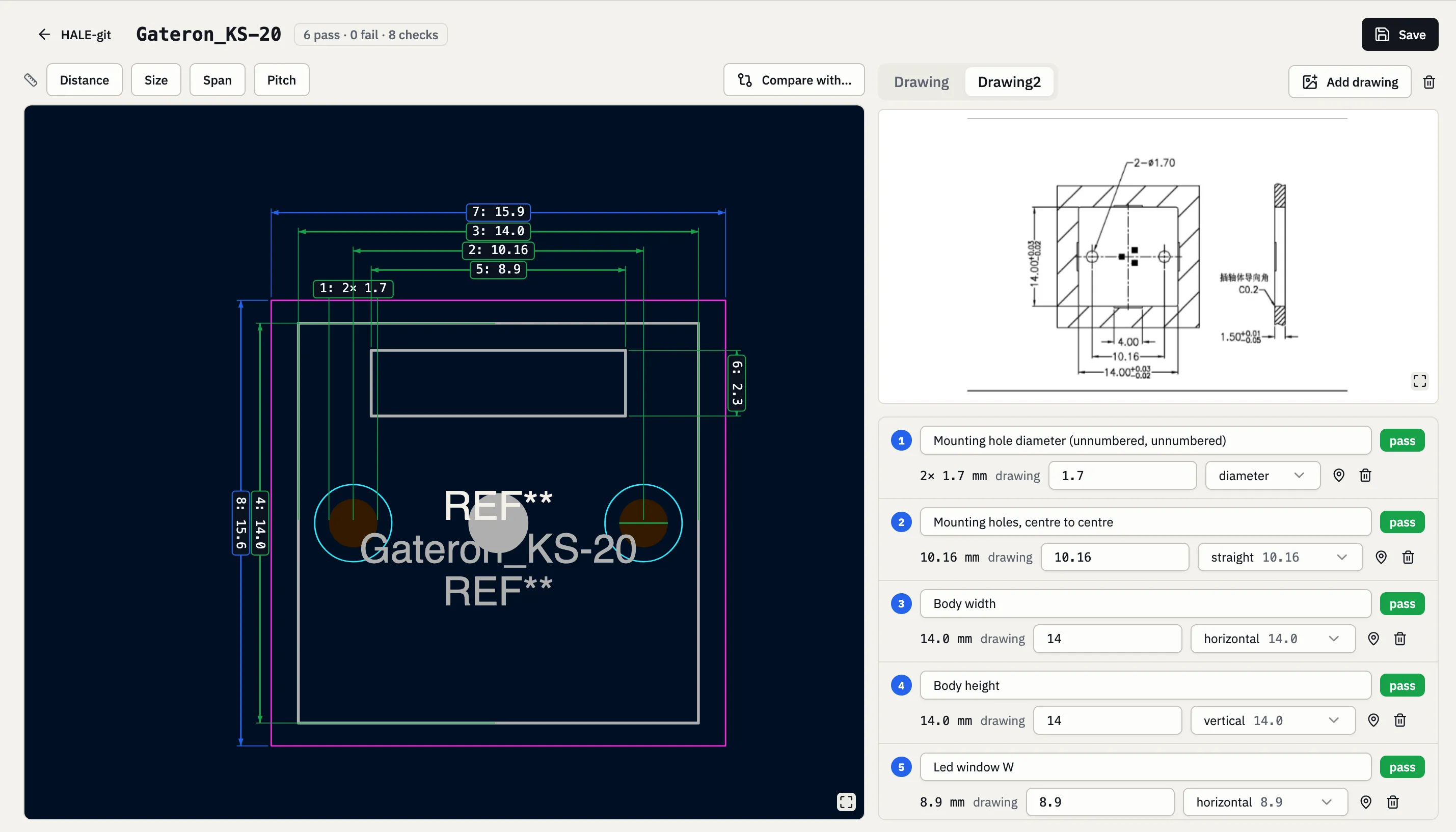
I also wanted to check how far off I was from the stock DRV5055 and SS39ET footprints. They felt too close to each other, so I compared them against each other, and they have effectively the same footprint in KiCad.
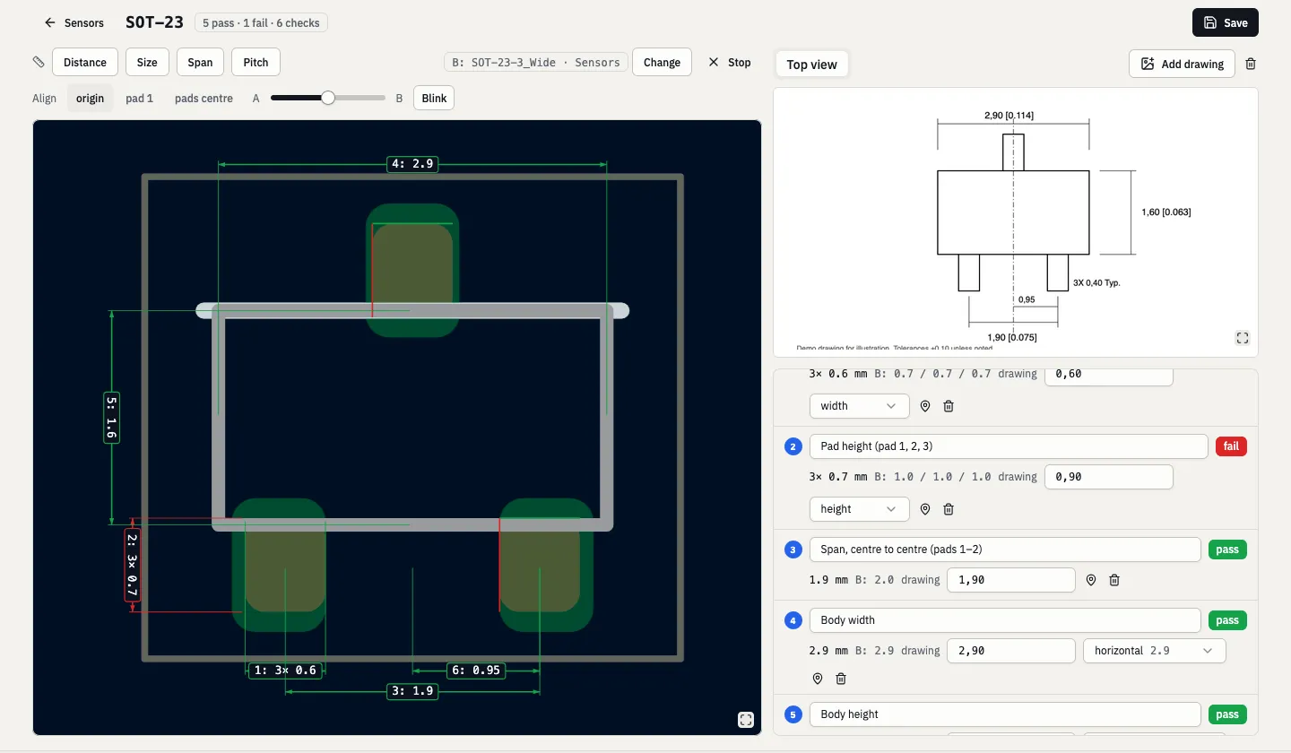
Assigning 3D models to the footprints and moving library items between libraries also needed some fixes and new UI.
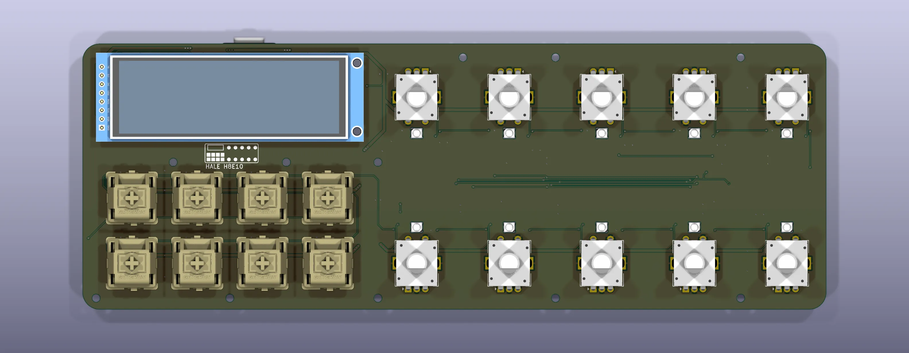
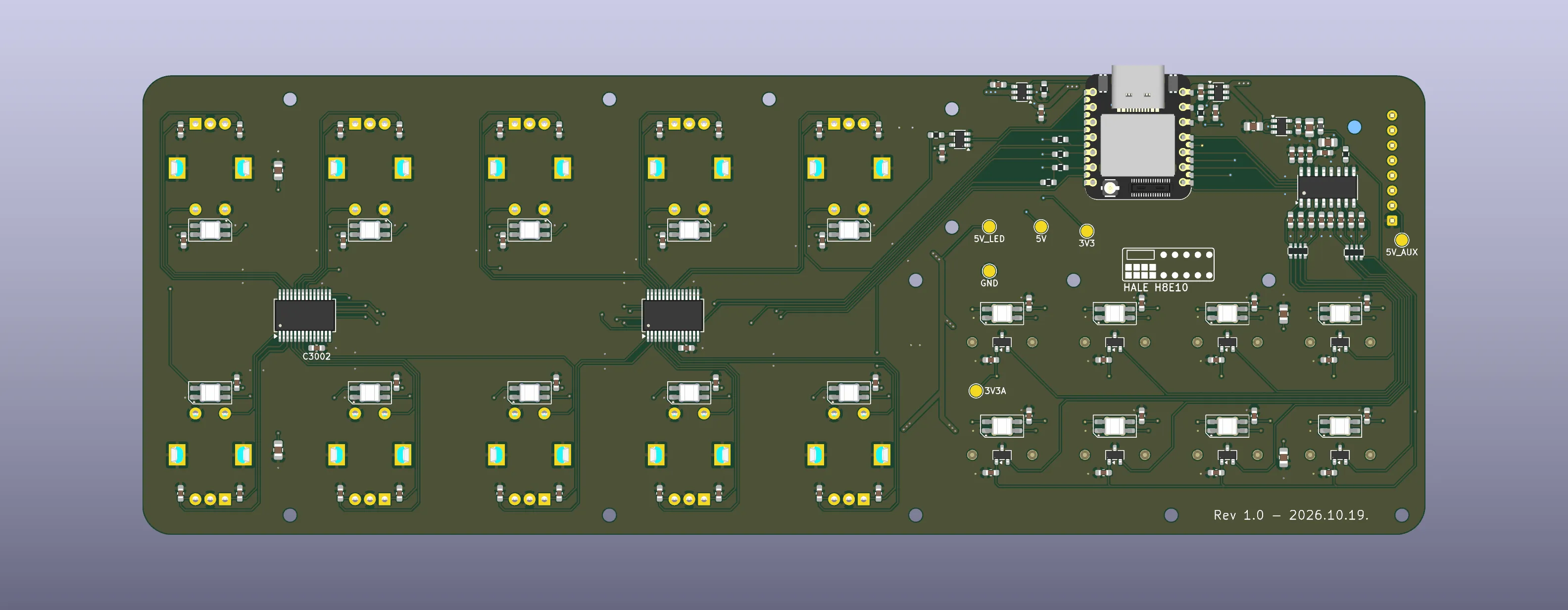
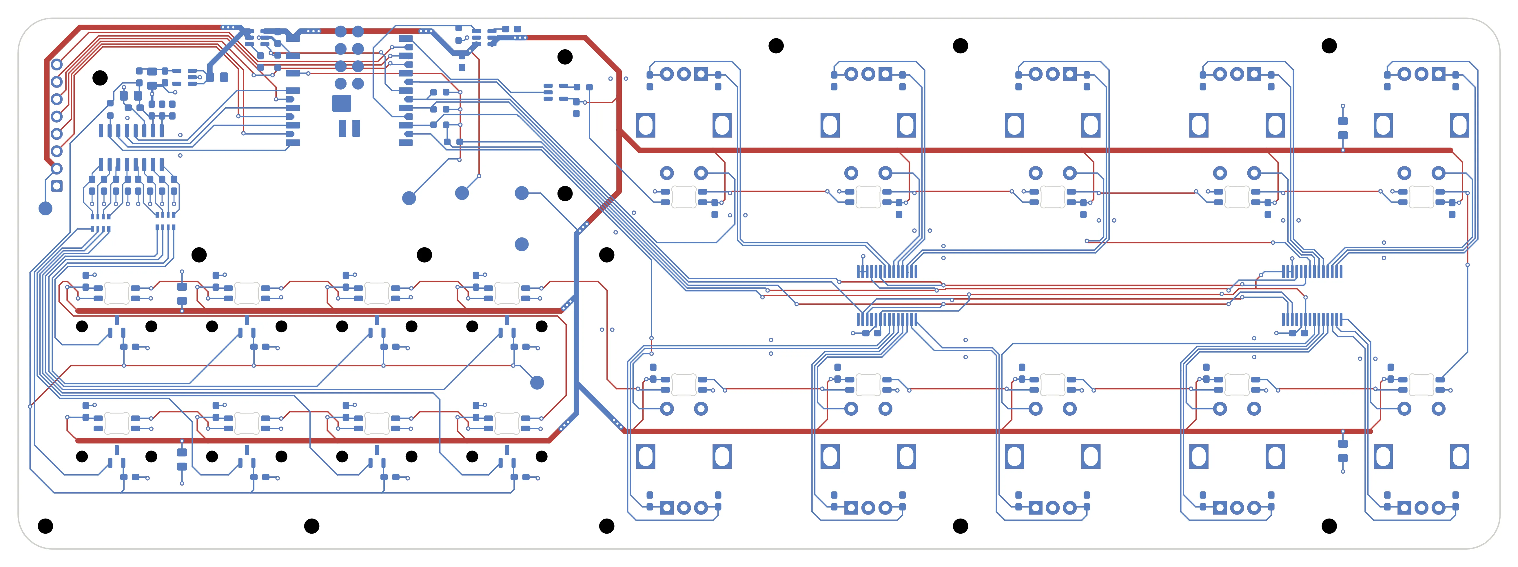
Drawing the PCB itself and organizing stuff was totally okay. I learned the Multi Channel tool from Claude. It works really well, and we will probably include it in our next tutorial.
The workflow was:
- get the coordinates from Claude, draw the board outline, move the keys, encoders and screen to the given positions and lock them
- wire up a single switch and a single encoder, then multi-channel copy them around to the already locked keys/encoders, and iterate on the “cells” a few rounds until they had the needed vias and data/power tracks
- place the LDO and the ADC with their filters and caps, then the GPIO expanders, and wire the keys and the encoders to them (changing the schematic along the way for easier wiring)
- wire the ADC, LDO, encoder buttons and expanders to the MCU
- wire the level shifter to the LED data line, the LED data itself, and the 5V for the LEDs
Then I started to question why we have a 220µF capacitor on the 5V line for the LEDs, whether we need it, and whether it could cause problems.
As I learned, there is a thing called inrush (I knew this was a thing: when you plug in a board, its caps start charging and look like a short circuit to the host). What I didn’t know is that the USB 2.0 spec caps the capacitance a device may present on VBUS at plug-in at 10µF, and the host needs at least 120µF on each port to absorb hot-plug inrush. If I add a 220µF cap to the 5V rail, at plug-in it pulls the host’s VBUS down, which can disturb other devices on the same host, trip the host’s over-current protection, or my device could simply get disconnected. So I started to count every cap on the 5V rail, and I had a LOT:
- 8.9µF inside the MCU module
- 10.1µF in the screen
- 18x 100nF next to the LEDs (1.8µF)
- 10µF before the analog rail LDO
- 220µF for the LED rail
If I drop the 220µF (which came from huge over-engineering anyway), it’s still ~30µF, and my LEDs need at least part of that 220µF back to keep them stable. Also, if the LEDs start to peak, they will drag the 5V rail down, and if it’s too much, the MCU could restart. So we had two potential problems: we were at least 3x over the allowed inrush, and we could starve the MCU.
(I started a small argument about USB inrush and over-engineering vs. price optimization, and there was a guy who had “never heard about this” and has a board with 60µF caps on the 5V rail without any problems :) )
So I introduced 2 load switches, which are probably not needed, but still much cheaper than trashing 5-10 test boards. I added one load switch for the LDO and the screen, and one for the LEDs. Now I can switch those rails on from the MCU, and those rails can’t brown out the MCU anymore, because if they try to draw too much current, the switch simply won’t give it to them. I also added 4x 10µF to my four LED lines. After I modified the schematic, it was easy to wire it up on the PCB. Now I have 10.9µF at plug-in (on paper still a little above the USB spec, but probably fine in reality), 20.1µF on the aux rail, and 41.8µF on the LED rail.
Claude drew a small logo for me, which I placed on both sides of the board. I also learned a more proper way to handle revisions and variables in the drawings.
The review phase
Some EEs reviewed my board. Mostly they said it looks fine, there are no big problems with it, it looks well thought out, no visible screw-ups.
One guy asked why I use load switches and a level shifter instead of discrete MOSFETs, but we agreed that the savings would be small, and sizing them correctly would be harder. After that, he said it would be sad if the sensors and the filters didn’t work as expected, and that started a feeling of anxiety.
H4E2
So after I lost my confidence and started to question every decision in my life, I realized the real risk: I can’t know if the sensor and filter choices work without real hardware. So I’d rather build a cheap board that tests exactly that. I copied the whole H8E10 project with save-as and started to “smart delete” things from it. I removed 4 keys, 8 encoders and 1 GPIO expander, which gives H4E2: 4 keys, 2 encoders. I also rerouted the keys to the ADC: every key is connected to the ADC with two wires, one filtered with an R and a C and one unfiltered, so I can test it with and without the filters. I will also order DRV5055A3QDBZRs, DRV5055A4QDBZRs and SS39ETs to test the different sensors.
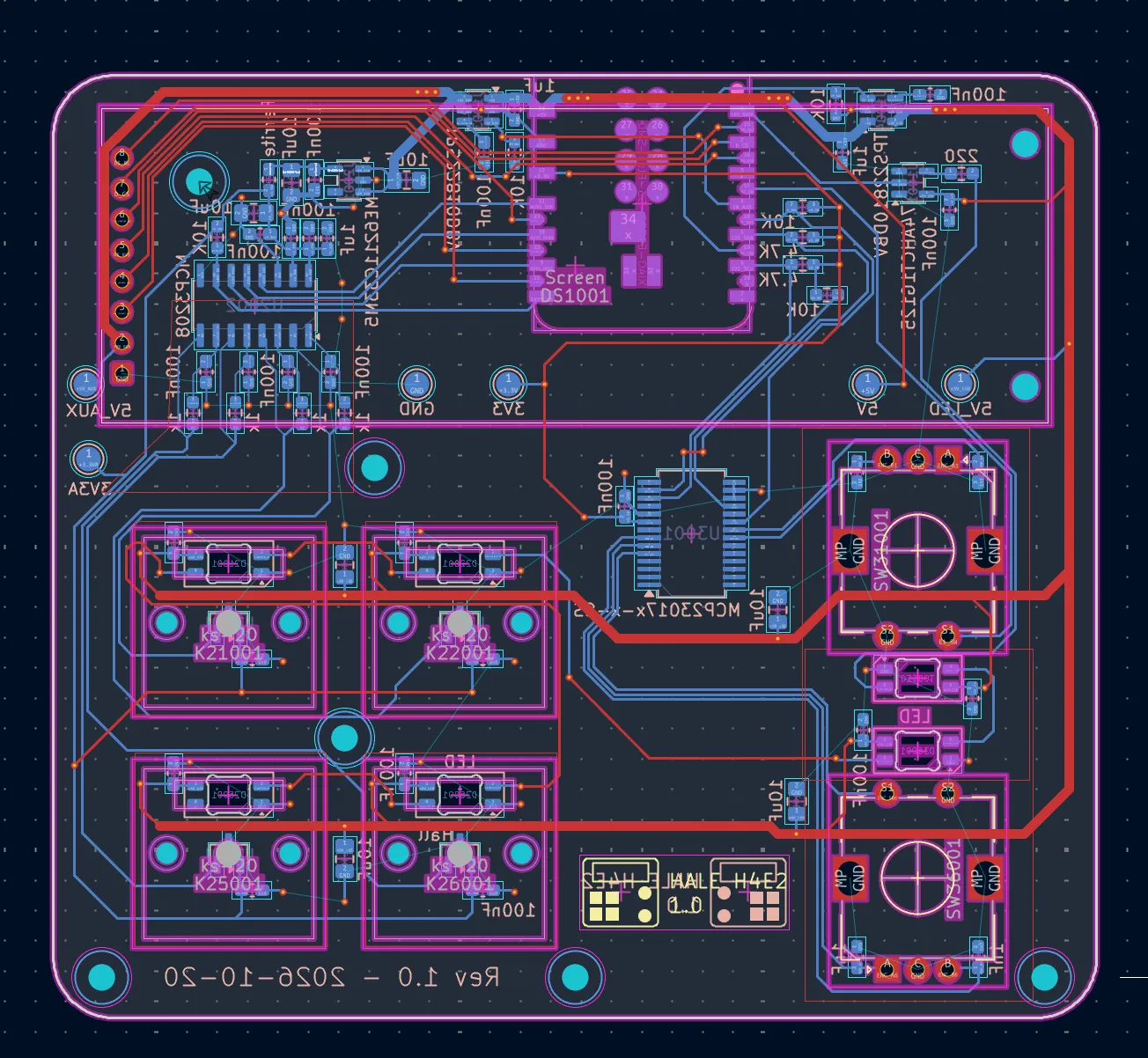
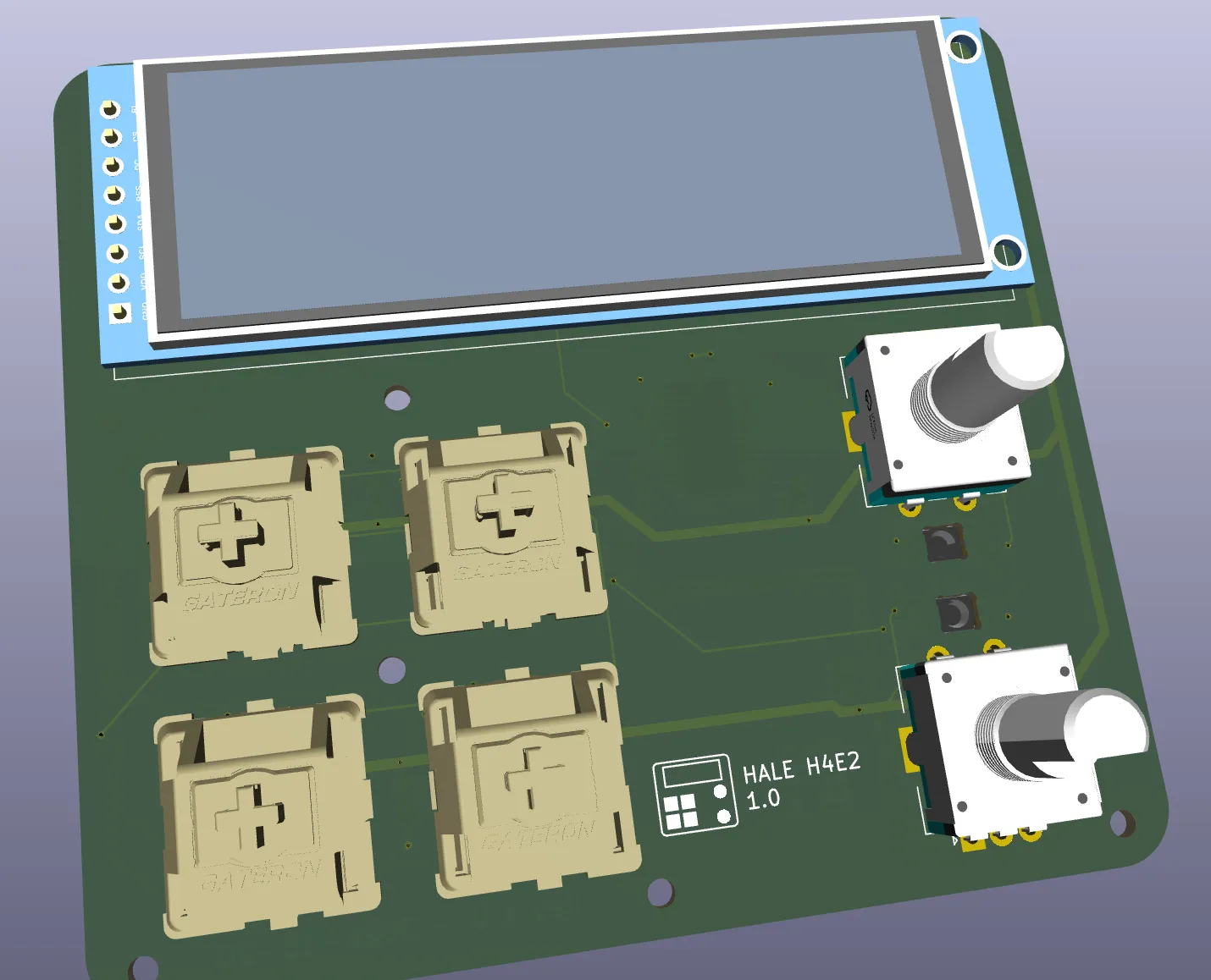
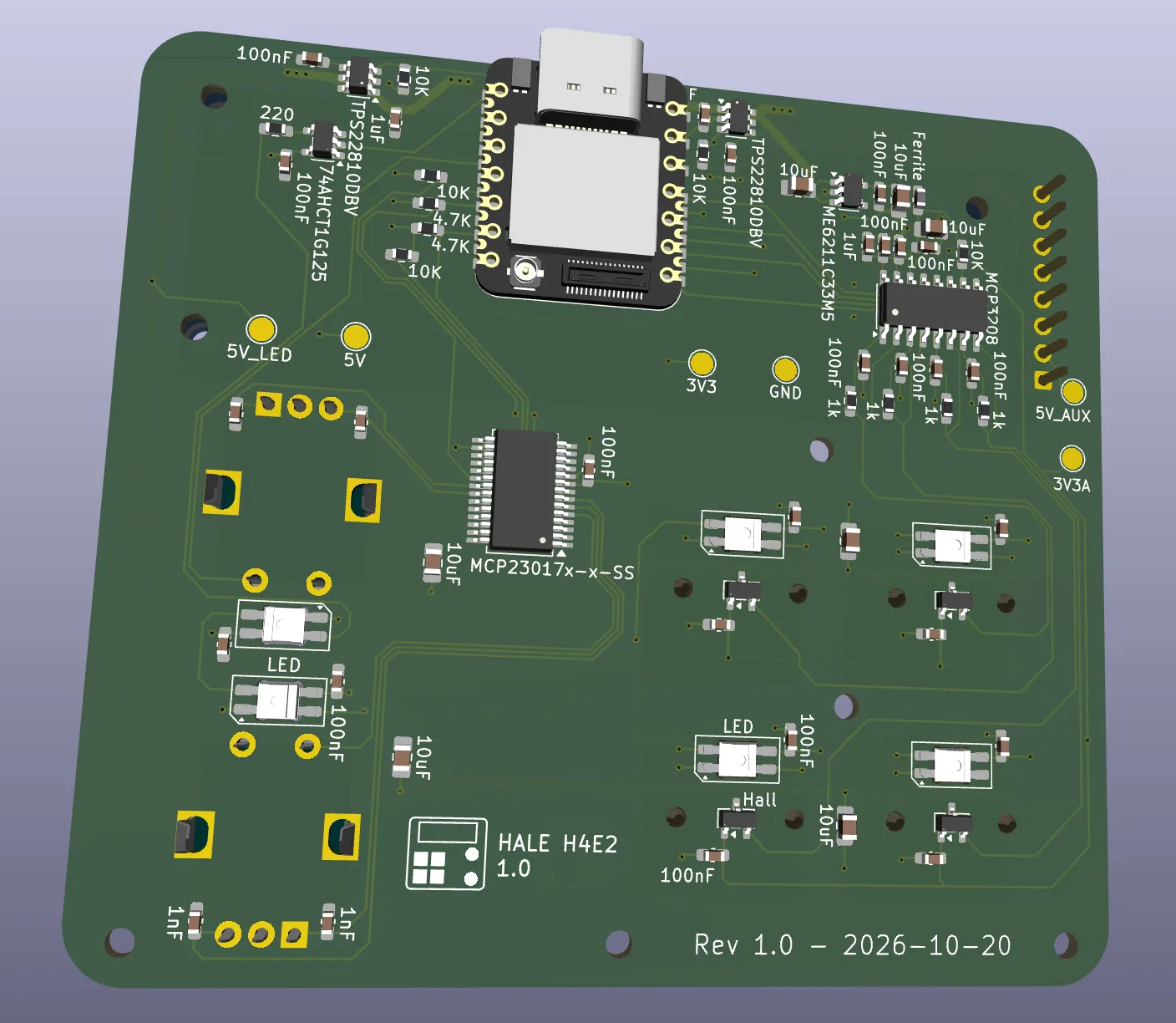
I will order this, one of my friends will hand-solder it, and we will see if everything works. I will also take some measurements with the different sensors, which will be interesting to see.
What I fixed in pcbjam along the way
Testing the platform was one of my three goals, and designing a whole board in it surfaced a few things that I fixed as I went:
- the symbol editor’s right-click menu didn’t show up
- creating a “new” symbol showed a strange error, even though it actually worked
- the library page said a lib had 0 items when it already had two
- I built and deployed a drawing comparison tool: you can save multiple drawings, draw reference measurements on them, and it helps you compare them against your footprint (more about it in last week’s devblog)
- you can now upload 3D models to a library and assign them to a footprint much more easily
- you can move library items between libraries
Conclusion
EE: I learned more in these weeks than in years of breadboarding. Mostly that a product isn’t a breadboard: the decoupling caps, pull-ups, inrush limits and load switches I’d never have added are what make a board survive being plugged in.
AI: helpful, with a clear split.
- Good at: ideation, explaining “why”, finding parts and OSS references, catching whole problem classes I didn’t know existed (inrush, ringing, sensor clipping), and being stricter than forum advice.
- Bad at: precise geometry. Reading a mechanical drawing, pin positions, exact distances. It produces things that look right. It also forgets context across sessions unless you write it down (CLAUDE.md, BOM.md).
- The real skill is asking the right question. The KS-20 problem surfaced “by chance”. Next time I’ll ask “what could make this not work?” at every step.
Rule I’m keeping: AI proposes, the datasheet decides. Measure everything that touches a drill hole.
pcbjam: I designed a whole board in it and fixed the things above along the way. The drawing comparison tool came straight out of this project. Otherwise it was totally okay to use. I don’t think desktop KiCad would have been significantly better.
Time-cost: about 34 hours in total.
- ~4h on the idea (on public transport, between sets in the gym, etc.)
- ~4h on data gathering and planning (models, datasheets, finding the sensor problem)
- ~4h on the initial schematic, symbols and footprints (without the platform fixes; I draw slowly, and I read most of the datasheets here)
- ~12h on the PCB
- ~4h on the wrap-up (chatting with EEs, writing this post, etc.)
- ~6h on the H4E2 (copy the project, delete things, modify/reposition the schematic and the PCB, new case)
Next: H4E2 gets ordered and hand-soldered, we measure the three sensors with and without filtering, and the case gets finished. That’s part 2.